Underst HDI PCB anding HDI PCB and Its Advantages
HDI PCB, also known as High Density Interconnect PCB, is a complex layered printed circuit board (CLPCB) that utilizes advanced circuit board technology (ACBT). It is designed to provide high interconnection density with fine-line printed circuitry. HDI PCBs are widely used in various industries due to their numerous advantages.
Manufacturing Process:
The manufacturing

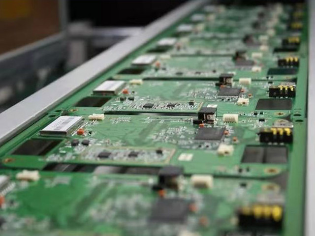
process of HDI PCB involves several steps. Firstly, the inner layer circuits are created by laminating multiple layers of copper foil onto an insulating substrate. These layers are then etched to form the desired circuit patterns. A dielectric material is applied over the inner layers, followed by the lamination of additional copper foils on outer surfaces. The outer layer circuits are patterned and etched through photolithogra HDI PCB phy processes. Finally, all layers are pressed together using heat and pressure to create the final product.
Characteristics:
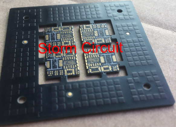
HDI PCBs exhibit several key characteristics that make them highly desirable in electro Aluminum PCB nic applications. Firstly, they offer higher connection densities compared to traditional multilayer PCBs since they employ microvias, blind vias, and buried vias to maximize space utilization. Additionally, these boards have finer line width and spacing capabilities due to advancements in manufacturing techniques. Furthermore, they possess exce HDI PCB llent electrical performance properties such as lower electrical noise levels and improved signal integrity.
Advantages:
The use of HDI PCBs provides numerous advantages for manufacturers and end-users alike. One significant advantage is their compact size which enables smaller electronic devices with enhanced functionality without compromising performance or reliability. Moreover, these boards offer improved thermal PCB supplier conductivity due Complex Layered Printed Circuit Board (CLPCB) to the use of materials like aluminum which dissipate heat efficiently during operation.
Furthermore, because HDI PCBs require fewer component connections than conventional designs—thanks to their increased interconnection density—the overall system cost can be significantly reduced.
Usage Guide:
To utilize an HDI PCB effectively, it is essential to follow a few guidelines. Firstly, when designing a circuit, it is important to consider th Advanced Circuit Board Technology (ACBT) e component placement and routing strategy carefully. Taking advantage of the smaller board size can help optimize signal integrity and minimize electromagnetic interference. S Fine-line printed circuit board econdly, while assembling components onto an HDI PCB, attention should be given to thermal management techniques since compact designs may generate more heat.
Selecting the Right Supplier:
When selecting an HDI PCB supplier, it is crucial to consider several factors. Reputation and experience are critical indicators of reliability and quality. It is
advisable to choose a supplier who has ample experience in manufacturing high-quality HDI PCBs and possesses certifications such as ISO 9001 or ISO 13485 for medical applications. Additionally, responsiveness in terms of customer support and prompt del
ivery capabilities should also be taken into consideration.
In conclusion, HDI PCBs offer advanced circuit board technology with exceptional density and performance capabilities. Their manufacturing process involves multiple layers and special vias that allow higher connection densities on a smaller form factor. By understanding its characteristics, advantages, usage methods, and how to select the right product supplier, one can harness the full potential of HDI PCBs in their electronic applications.
Remember: when it comes to complex layered printed circuit boards – th Multilayer PCB ink High Density Interconnect!